The full name of TFT is Thin Film Transistor (thin film field effect transistor), which means that each liquid crystal pixel on the liquid crystal display is driven by a thin film transistor integrated behind it, so that a high-speed, high-brightness, high-contrast display screen can be achieved. Information, TFT is an active matrix liquid crystal display, and TFT-LCD (Thin Film Transistor Liquid Crystal Display) is a type of most liquid crystal displays.
Youritech offers a range of TFT display options that meet industrial standards, including modules such as IPS TFT, High Brightness TFT LCD (sunlight readable), Bar Type TFT, Wide Temperature TFT LCD, and others. These displays can be used in landscape or portrait orientations and come in both Mono and full-color options with various resolutions. Touch screen capabilities are available in resistive and projected capacitive (PCAP touch screen) technologies. These display modules support multiple interfaces such as MCU, RGB, TTL, LVDS, and MIPI DSI, making them versatile for applications in industrial control, medical equipment, POS systems, automation, GPS navigation, and more.
High display quality
TFT with Full Range of Viewing Angles
Wide Application Range of TFT-LCD Display
Wide Use of Application Temperature
Good Color Performance
Low Power Consumption
Televisions and home theater systems
Gaming consoles
Medical monitors
Automotive infotainment systems
Industrial human-machine interfaces
Public information displays
Consumer electronics products
Automobile industry
Medical equipment
Aerospace
Industrial applications.
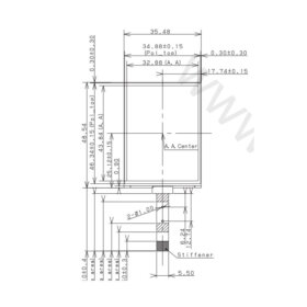
TM185VDSG06 Displays
TM185VDSG06 Original 18.5 Inch 1920x1080 eDP TFT LCD Display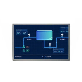
TM185VDSG07 Displays
TM185VDSG07 Original 18.5 Inch 1024x768 LVDS TFT LCD Display
TM150TDSG81 TFT Display
TM150TDSG81 Original 15 Inch 1024x768 eDP TFT LCD Display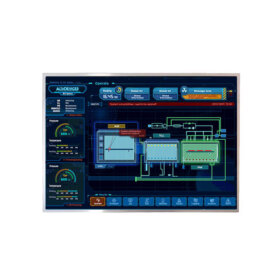
P1210XGF1MA01 LCD Display
P1210XGF1MA01 Original 12.1 Inch 1024x768 High Brightness Wide Temperature TFT LCD Display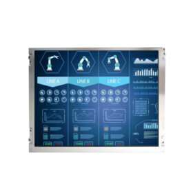
P1210SVF1MB00 Displays
P1210SVF1MB00 Original 12.1 Inch 800x600 LVDS TFT LCD Display
TM104TDGP13-00 Displays
P1040XGF1MA00 Original 10.4 Inch 1024x768 Ultra High Brightness Wide Temperature TFT LCD Display
P0840XGF1MB00 Displays
P0840XGF1MB00 Original 8.4 Inch 1024x768 High Brightness Wide Temperature TFT LCD Display
P0840SVN1MB00 Displays
P0840SVN1MB00 Original 8.4 Inch TFT LCD Display 800x600 LVDS LCD Module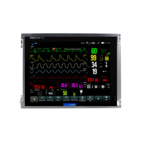
TM104SDH02 Displays
TM104SDH02 Tianma 10.4 Inch 800x600 Wide Temperature LVDS LCD Display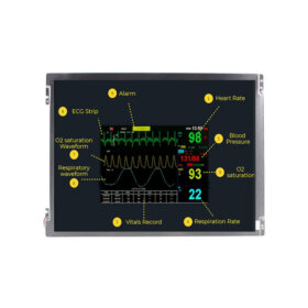
TM104SDH01-00 Displays
TM104SDH01-00 Tianma 10.4 Inch TFT LCD Display 800x600 LVDS LCD Module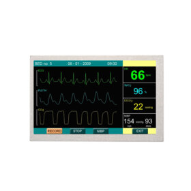
TM101JDHG32-00 LCD Display
TM101JDHG32-00 Tianma 10.1 Inch TFT LCD Display 1280x800 Ultra High Brightness LCD Display
TM101JDHP03-00 TFT Display
TM101JDHP03-00 Tianma 10.1 Inch TFT LCD Display 1280x800 LVDS LCD Module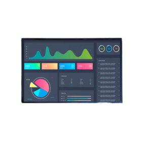
TM101JDHG38-00 Displays
TM101JDHG38-00 Tianma 10.1 Inch TFT LCD Display 1280x800 LVDS LCD Module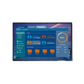
TM101JDHP01-00 Displays
TM101JDHP01-00 Tianma 10.1 Inch TFT LCD Display 1280x800 LVDS LCD Module
P1010WSN1ME00 Displays
P1010WSN1ME00 Tianma 10.1 Inch TFT LCD Display 1024×600 LVDS LCD Module
TM084SDHG01-01 Displays
TM084SDHG01-01 Tianma 8.4 Inch TFT LCD Display 800x600 LVDS LCD Module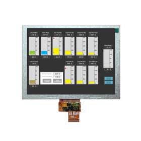
TM080TDGP02-00 TFT Display
TM080TDGP02-00 Tianma 8 Inch TFT LCD Display 1024×768 LVDS LCD Module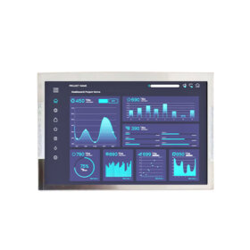
P0700WVF1MA00 TFT Display
P0700WVF1MA00 Tianma 7 Inch TFT LCD Display 800×480 Sunlight Readable LVDS LCD Module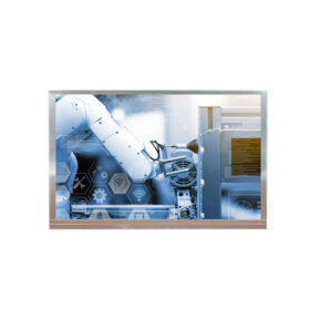
TM070RDSG12-00 Displays
TM070RDSG12-00 Tianma 7 Inch TFT LCD Display 800×480 LVDS LCD Module
P0700WVN1MB01 Displays
P0700WVN1MB01 Tianma 7 Inch TFT LCD Display 800x480 TTL LCD Module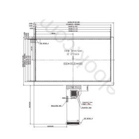
P0700WVN1ME01 Displays
P0700WVN1ME01 Tianma 7 Inch TFT LCD Display 800x480 Parallel RGB LCD Module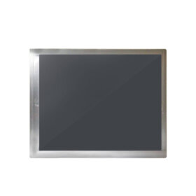
P0650VGF1MA10 Displays
P0650VGF1MA10 Tianma 6.5 Inch TFT LCD Display 640×480 Sunlight Readable LVDS LCD Module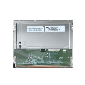
P0650VGF1MA00 IPS Display
P0650VGF1MA00 Tianma Original 6.5 Inch TFT LCD Display 640x480 Sunlight Readable LVDS LCD Module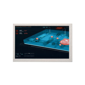
LQ190E1LX76 Displays
LQ190E1LX76 Sharp 19 Inch TFT LCD Display 1280×1024 LVDS LCD Screen For Industrial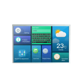
LS121K1LX02 TFT Display
LS121K1LX02 Sharp 12.1 Inch TFT LCD Display 1280×800 LVDS LCD Module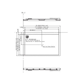
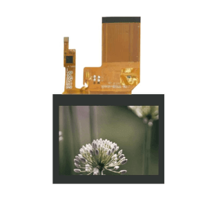
LS022B7DH03 IPS Display
LS022B7DH03 Sharp 2.2 Inch TFT LCD Display 240x320 Transflective 3-wire SPI LCD Module
COM104H9M25SSS Displays
COM104H9M25SSS Original 10.4 Inch TFT LCD Display 800×600 LVDS Sunlight Readable LCD Panel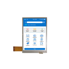

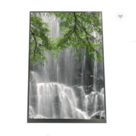
ET185FH01-OT Displays
Factory OEM ODM 18.5 Inch TFT LCD Display USB LCD Panel With Touch Display
ET070WU12-O Displays
Factory Custom 7 Inch TFT LCD Display 1200×1920 MIPI High Brightness LCD Panel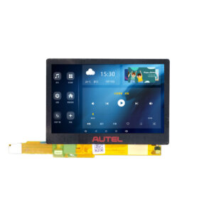
ET041HD03-OT TFT Display
Factory OEM ODM 4.13 Inch TFT LCD Display 1200×720 MIPI LCD Panel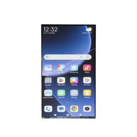
ET070WV02-CT Displays
Factory OEM ODM 7 Inch TFT LCD Display 800×480 LVDS High Brightness LCD Panel
ET070WX05-OT Displays
OEM ODM 7 Inch TFT LCD Display 800×1280 MIPI LCD Panel For Industrial
ET070WU07-OT IPS Display
Factory OEM ODM 7 Inch TFT LCD Display 1200×1920 MIPI LCD Panel
ET070WU11-OT LCD Display
Factory Custom 7 Inch TFT LCD Display 1200×1920 MIPI LCD Panel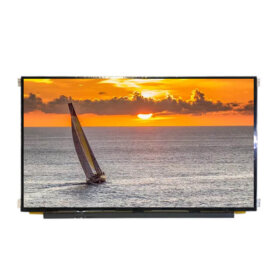 ET156D1JW31 3840x2160 15.6 inch laptop display 40 pins 4k lcd module IPS display
 3.5inch ips lcd full viewing angle 640x480 lcd MIPI RGB interface landscape 3.5" tft panel
 10.1inch custom lcde 1200x1920 display mipi interface 10.1" ips lcd screen full viewing angl
 high quality 10.1 inch 1920x1200 IPS TFT LCD display WITH LVDS (2ch) 40pin interface for medical
 7 inch ips lvds tft 1280x800 40pins LVDS WLED TFT LCD Display with wide viewing angel
 ET156Z1JW01 15.6 inch LCD panel 3200x1800 QHD IPS LCD Display for Laptop
 ET133DSE-GP1 13.3 4K LCD 3840x2160 IPS EDP 40 PIN 72%NTSC Lcd Screen Module
 ET024QV02-V 2.4inch LCD 240*320 resolution ST7789V IC TN MODE cheapest
 COM20T2P31ILC Ortustech 2 Inch TFT LCD Display 240×320 CPU/RGB/SPI LCD Panel